GTB Usage and Successful Stories
GTB Introduction
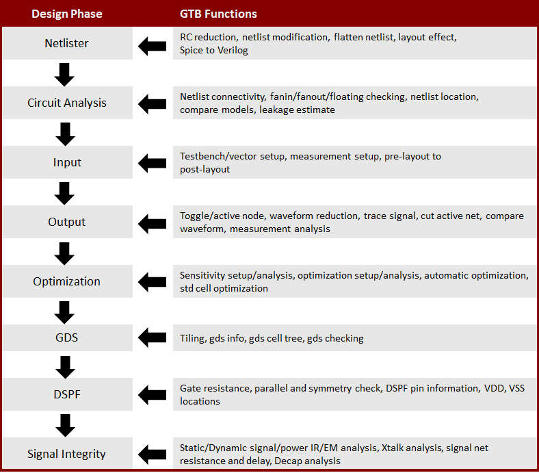
GTB (G-Analog Tool Box) is a new class of custom circuit design tool with a collection of over 80 tools and each tool addresses different aspect of the custom circuit design process. The main focus is on ease of use, improving designer efficiency and improving product quality.
Custom circuit design process mainly consists of loosely coupled tools, such as schematic, simulation, layout, verification and extraction. Interfaces between tools are defined by industry standard file formats, such as Spice netlist, GDS, DSPF file formats. Other specialized tools are also needed to set up, optimize, translate and analyze the design database. Custom circuit design tools are complicated and hard to learn and use. Designers spend lots of time setting up the analysis and analyzing the results. The custom circuit design process can be greatly improved by adding more automation and easy to use tool sets that improve the efficiency in the design process. GTB consists of more than 80 easy to use tools that improve the efficiency and quality of custom circuit design process.
GTB Automating a Variety of Tasks in Custom Design Flow
GTB Applications:
- Netlist modification and translation
- Netlist analysis and checking
- Simulation input setup
- Simulation output analysis
- Circuit checking
- Circuit debugging
- Data Processing
- Circuit sensitivity analysis / optimization
- Signal integrity analysis
- Post-layout effect analysis and checking
- GDS utility and checking
Easy to Use Intuitive GTB GUI
GTB Usages and Success Stories:
GTB contains more than 80 different functions for custom circuit design, they can be used at different stages of the design process and they work with different input formats. Here are some of the tool usage by customers.
Perform Full Chip Simulation with Verilog
Designer needs to perform full chip function simulation of a memory test chip. Traditional fast Spice simulator will take 10’s of years to simulate. Using the “Spice to Verilog” function, the designer can convert the CDL netlist to a switch/gate level Verilog netlist. After replacing I/O, memory array and sense amp with vendor and custom Verilog modules. The full chip function simulation can be finished within hours.
Perform Post-layout ECO
Designer needs to make design changes to memory macro to satisfy design requirements. Before committing layout changes, the designer needs to know whether the new post-layout simulation can satisfy design requirements after layout changes. Using the “Post-layout ECO” function, the designer can generate a new DSPF post-layout netlist which contains the intended changes. The designer can then run simulation to verify whether the design changes can satisfy the design requirements.
Uniquify Netlist
Designer needs to deliver CDL netlist of an IP. The netlist needs to be hierarchical but hide the schematic names. Using the “Uniquify netlist” function, the designer can create a new netlist using numbers as cell names. If needed, the cells can be selectively flattened using the function “Flatten cell”
Find All Instance Locations in a Chip
Designer needs to build bitmap for a memory test chip. The test chip has 128 instances of identical memory macro. Using the “LVS netlist location” function, the designer can find the location and rotation of each memory macro from the LVS generated layout netlist. Combined with the bitmap within the macro, the designer can then create the full chip bitmap.
Vector Generation
Designer needs to perform exhaustive function verification of a memory IP using fast Spice simulator. Designer needs to create vector file that cover the function space. Using the “Vector generation” function, the designer can generate the Spice vector file to verify the functionality of the memory IP.
Reduce Post-layout Simulation Results Size
Designer needs to reduce the output file size of post-layout simulation when all nodes are printed out for debugging. Using the “Output Statement Reduction” function, the designer can obtain a set of output statements which only print out one node for each net. This will greatly reduce the output file size, the node names will also be converted to hierarchical names so that they can be easily navigated in waveform display tool. For an output file which contains the waveforms of every node of a post-layout netlist, it can also be reduced. Using the function “Waveform reduction”, the designer can generate a new waveform file which contains the waveform of only one node for each net.
Generate PWL Statements from Waveform File
Designer needs to extract the waveform of some signals into PWL voltage statements, so that they can be used for other simulation. Using the function “Waveform to PWL”, designer can convert the selected signal waveforms into PWL voltage sources.
Extract A Block Netlist and Stimuli for Detailed Analysis
The designer finds a block behaves incorrectly in simulation. In order to do further analyze and optimize the block. It’s necessary to extract the block netlist and input stimuli to perform further simulation. Using the function “Cut critical block” for pre-layout or post-layout netlist, the designer can obtain a standalone simulation deck which contains the netlist and stimuli of the block. The designer can perform more detailed analysis of the block to identify the problem.
Tabulate and Analyze Measurement Results
Designer needs to display measurement results side by side from different simulations. The simulations are obtained from either using .data or .alter statements. Using the function “Tabulate measurement”, the designer can display measurement results from different simulations in a tabular format for easy viewing. Using the function “Measurement analysis”, the designer can view measurement differences between different simulations. The designer can also use the filter function to display the results satisfying user specified criteria for circuit optimization.
Select Design Variables and Set Up Simulation Test bench
Designer needs to select design variables in the netlist and setup simulation testbench for circuit optimization. Using the function “Test circuit setup”, the designer can select the design variables and ranges of the variables from a testbench and the function will generate a new testbench for simulation. This function is similar to Cadence Virtuoso ADE except it uses netlist as input instead of schematic. The simulation results can be analyzed by the function “Test results analysis”.
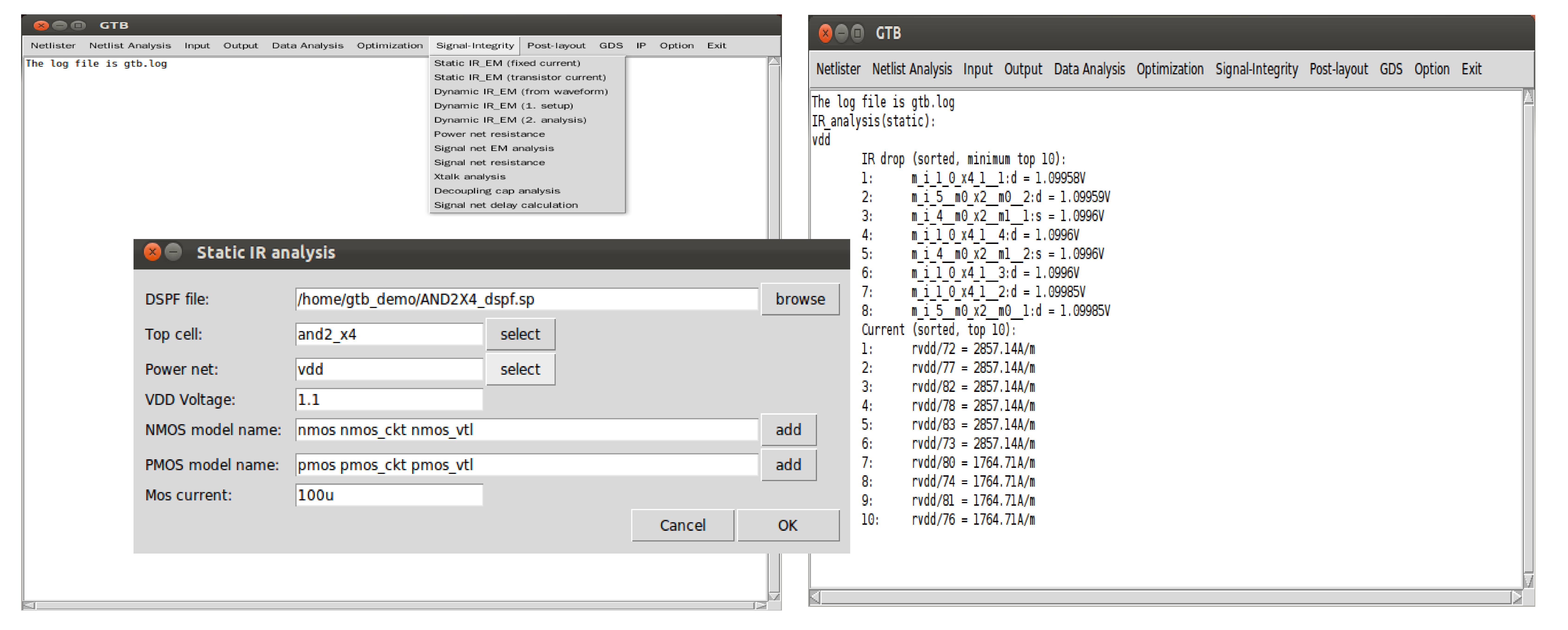
Perform Power Network IR Analysis
Designer needs to perform fast static IR drop analysis on a block or a macro. Using the function “Static IR_EM (fixed current)”, the designer assign a static transistor current to each transistor connected to either VDD or VSS. The function reads in the post-layout DSPF file which contains parasitic resistor location, layer and width. The graphical output result temperature map which shows the severity of the IR/EM can be displayed by the public domain tool, klayout. The text output results are sorted by severity. The function can handle up to 20M resistors, enough to handle largest IP macro or a small chip up to few mm^2. Instead of using fixed transistor current, designer can also use the function “Static IR_EM (transistor current) to calculate the IR/EM using simulated transistor current. Sometimes, designer also need to calculate the equivalent resistance of a node within the power network. Using the function “Power net resistance”, designer can calculate the equivalent resistance of a node within the power network.
Calculate Signal Net Resistance and Delay
Designer needs to calculate the parasitic resistance and delay of the signal nets to check long wire with large resistance and long delay. Using the function “Signal net resistance”, designer can get the largest resistance of each net. Designer can also calculate from only one source node and select the top level nodes. Using the function “Signal net delay”, the function will also calculate the delay in the signal net parasitic.
Perform Cross Talk Analysis
Designer needs to perform cross talk analysis to check for potential cross talk issue. Using the function “Xtalk analysis(Static)”, the function can find potential cross talk issue based on total couple ratio and individual couple ratio. If the simulation results are available then designer can use the function “Xtalk analysis(dynamic)” to perform vector based cross talk analysis. The function will use the transition window to determine whether cross talk occur or not.
Display Signal Layout Routing
Designer needs to optimize and match routing resistance of a MUX circuit layout. Using the function “Create DSPF Net GDS”, designer can display layout routing of each signal net. By comparing the routing of each signal path in the MUX layout, designer can better optimize the layout. Designer can also use the function “Signal net resistance” to calculate the resistance of each net which also help designer to optimize the layout.
GDS Tiling
Designer needs to tile standard cell layout together to perform DRC check. Using the function “Tiling tool”, designer can tile a layout cell into different tiling patterns to run DRC.